| Serie | VCB48_QBO-600WR3A(D)-N |
|---|
| Modell | VCB4810QBO-600WR3A-N |
|---|
| Typ | DC/DC-Wandler |
|---|
| Marke | MORNSUN |
|---|
| Input Current (full load) | 16A max (Room temperature, Vin = 40 V) |
|---|
| No Load Input Loss | 9.7W (Room temperature, Vin = 53 V) |
|---|
| Input Capacitance Value | 5µF (Room temperature, Vin = 53 V) |
|---|
| Surge Voltage(100msec. max.) | -0.5–80 (Room temperature) |
|---|
| Max input Voltage | Room temperature: 65 VDC; Output voltage enabled level, PMBus: VDC |
|---|
| Input Start-up Voltage ④ | 36–38 (configurable; Output voltage disabled level, PMBus) |
|---|
| Input Under-voltage Protection | 34–36 (configurable) |
|---|
| Eingangsfilter | Pi filter; Unavailable, it is necessary to ensure that the |
|---|
| Hot-Plug | input and output capacitors without voltage; before loading and unloading the product |
|---|
| Module turn-on | 0–1.2 (Room temperature) |
|---|
| Module turn-off | 2.5–5.5 VDC (Room temperature) |
|---|
| CTRL flip typical value | 1.7 |
|---|
| Input current ② | 0.3mA |
|---|
| Input loss during shutdown | 1W (Room temperature, Vin = 53 V) |
|---|
| | 1 (T) |
|---|
| Functional delay time | 1 ③: ms; Room: 11 ms typ, 20 ms max; VCB48_QBO-600WR3A-N ⑤: ms |
|---|
| Start-up Delay Time | 201 typ, 210 max (VCB48_QBO-600WR3D-N) (2 ③; Vin = 53 V) |
|---|
| Output Current Range | 0–100 %Io; Room temperature, VCB48_QBO-600WR3A-N: ±2 %Io max |
|---|
| Ausgangsspannungsgenauigkeit | ±2% (0%-100%Io VCB48_QBO-600WR3D-N) (Vin = 40-60 V,) |
|---|
| Lineare Regelung | Vin = 40-60 V, 100%Io: ±0.2% typ, ±0.5% max; Room temperature,: % |
|---|
| Lastregelung | ±0.5 typ, ±0.75 max (Vin = 53 V, VCB48_QBO-600WR3A-N ⑫) (0%-100%Io) |
|---|
| Transient Recovery Time | Vin = 53 V, 25-75-25% Io, di/dt = 2.5 A/μs: 250 µs typ, 450 µs max; Vin = 53 V, 25-75-25% Io, di/dt = 2.5 A/μs: ±3 µs typ, ±4 µs max |
|---|
| Transient Response Deviation | %; Vin = 53 V, 10-100-10% Io, di/dt = 2.5 A/μs: ±15% |
|---|
| Temperaturkoeffizient | 100%Io: ±0.03%/℃; Room temperature,: %/℃ |
|---|
| Ripple & Noise ② | 100mVp-p max; Vin = 40-60 V, 0%-100%Io: mVp-p; Room temperature,: mVp-p |
|---|
| Output Voltage Regulation range ③ | 8–13.2 VDC; Vin = 40-60 V, 0%-100%Io: VDC |
|---|
| Übertemperaturschutz | Product surface max. temperature: 110℃ typ, 120℃ max; Vin = 40-60 V: 130 %Vo |
|---|
| Überspannungsschutz | Response type: Output off, re-power on for recover A; Vin = 40-60 V: 65A typ, 70A max; VCB48_QBO-600WR3A-N: ①Hiccup, continuous, self-recovery A |
|---|
| Überstromschutz | Response type: ②The minimum current limit for a group of N; devices in parallel is 89.5A*N (VCB48_QBO-600WR3D-N; VCB48_QBO-600WR3A-N) |
|---|
| Kurzschlussschutz | Vin = 40-60 V: Hiccup, continuous, self-recovery; Vin = 53 V, VCB48_QBO-600WR3A-N: 50 typ, 70 max (VCB48_QBO-600WR3D-N) |
|---|
| 3 | 240 typ, 260 max (resistance load VCB48_QBO-600WR3D-N) |
|---|
| Initialization time | From Vin ≥27V to ready enable: 18; The input voltage is enabled: 40 |
|---|
| Delay Time | Enable by CTRL or PMBus CTRL pin: 1; Default startup delay of PMBus: 1 |
|---|
| Output Voltage On Delay Time ⑤ | TON_DELAY range: 0–655 ms; Accuracy (actual delay and set value): 1 ms; Default off delay of PMBus: 1 ms |
|---|
| Output Voltage Off Delay Time ⑥ | TOFF_DELAY range: 0–655; Accuracy (actual delay and set value): 1; Room VCB48_QBO-600WR3A-N ⑦: 10 typ, 15 max |
|---|
| 4 | VCB48_QBO-600WR3D-N ⑧: 200 typ, 210 max; Room VCB48_QBO-600WR3A-N: 15 (0%-100%Io) |
|---|
| Abnormal Fault Time ⑨ | 210 (0%-100%Io VCB48_QBO-600WR3D-N) |
|---|
| Output Voltage Drop Time ⑩ | Room temperature, 0%-100%Io: 10; TON_RISE/TOFF_FALL range: 10–655 |
|---|
| The Output Voltage Rises/Falls | 1; Default output voltage adjustment rate of PMBus: 0.1 (Accuracy of rise/fall time (actual rise/fall time and; set value)) |
|---|
| Output Voltage Adjustment Rate ⑪ | V/ms; VOUT_TRANSITION_RATE range room temperature,: V/ms; 0.001–1.2 V/ms; 0%-100%Io, no current sharing, no parallel: V/ms |
|---|
| Isolation (Eingang–Ausgang) | 1500 VDC (Electric Strength Test for 1 Input-output) |
|---|
| Isolation | VDC (minute with a leakage) |
|---|
| Isolationswiderstand | Input-output, resistance at 500VDC: 100 MΩ |
|---|
| Isolationskapazität | 8200 pF (Input-output, 100KHz/0.1V) |
|---|
| Betriebstemperatur | -40 to +85℃ |
|---|
| Lagertemperatur | -55–+125℃ |
|---|
| Lagerfeuchtigkeit | 5–95 %RH (Non-condensing) |
|---|
| Gehäusematerial | Aluminum alloy case |
|---|
| Dimension | 58.4*36.8*: 14.2 mm |
|---|
| Gewicht | 85.8g (Typ.) |
|---|
| Kühlmethode | Free air convection cooling or forced air cooling |
|---|
| Typical Characteristic | Curve; Fig. 1 |
|---|
| 1. Typical application | circuit |
|---|
| The input voltage ranges | from 40 to 60VDC. When the input voltage exceeds 60VDC, the power loss is higher than the normal input |
|---|
| voltage. The maximum continuous | input voltage is 65VDC. |
|---|
| If the customer does not | use our EMC recommended circuits, the input must be connected with an electrolytic capacitor of at least |
|---|
| 470µF to suppress the potential | surge voltage at the input and ensure that the transient voltage does not exceed the value specified in the |
|---|
| In addition, the impedance | of both the input source and the load will interact with the impedance of the product, requiring the input |
|---|
| source to have a low impedance | characteristics. It is recommended that the minimum capacitance of the external input can be |
|---|
| guaranteed to be 470 µF at low | temperature. In some applications, performance can be enhanced by adding external capacitors. If the |
|---|
| input voltage source contains | significant inductance, add a low ESR ceramic capacitor of 22-100 µF to the input of the product to ensure |
|---|
| stable operation. The minimum | required capacitance depends on the output power and input voltage. The higher the output power, the |
|---|
| The output end must be | connected with an electrolytic capacitor larger than the minimum capacitive load capacity to stabilize the |
|---|
| If it is required to further | reduce the input/output ripple, the external input/output capacitors Cin and Cout can be increased or a |
|---|
| capacitor with small series | equivalent impedance value can be selected, but the capacitance value should not be greater than the |
|---|
| maximum capacitive load of | the product.; Capacitors |
|---|
| +Vin | +Vo Output Value Cout (typ.) Cin; Voltage |
|---|
| Cin DC | DC; Cout; 10.8/10.9/12/12.1V 2600µF ① /35V 470 µF/100V |
|---|
| -Vin | 0V; Fig. 2 ① It is recommended to carry out peripheral design according to the typical; value of capacitive load, and use aluminum electrolytic capacitors or solid; electrolytic capacitors. The ratio of capacitive value can be referred to:; 7x470µF + 270µF. |
|---|
| In addition to the 1. 5 7 19 1 0 5 127.32 602.91 25.55 10.22 100 Typical 5 7 19 1 0 6 154.92 602.91 43.75 10.22 100 Application 5 7 19 1 0 7 200.76 602.91 26.53 10.22 100 Circuit | capacitors, 10µF/35V tantalum capacitors and 0.1µF/25V ceramic capacitors should be |
|---|
| added to the ripple noise test. | It is recommended to use the following recommended peripheral circuit, and set the probe bandwidth to |
|---|
| 20MHz during the test. | Components Recommended Component; C0 470µF/100V electrolytic capacitors; C1 0.1µF/25V ceramic capacitance; C2 10µF/35V Tantalum capacitor; C3 2600µF/35V aluminum electrolytic; capacitor; Fig. 3 |
|---|
| 3. EMC compliance | circuit; Components Recommended Component; C01 680µF/100V electrolytic capacitors; C02 470µF/100V electrolytic capacitors; C03 470uF/35V electrolytic capacitors; C1 475K/100V ceramic capacitance; C2 4*475K/100V ceramic capacitance; C3 2*475K/100V ceramic capacitance; 300uH, recommended to use MORNSUN; LCM1; P/N: FL2D-C5-301; CY1/CY2 3*4.7nF/Y2; Fig. 4-1; Components Recommended Component; C01/C02 470uF/100V electrolytic capacitors; C03 3*1000uF/35V electrolytic capacitors; C1 475K/100V thin film capacitance; C2/C3/C4 225K/450V thin film capacitance; C5/C6 2*225K/450V thin film capacitance; CY1/CY2 2*4.7nF/Y2; CY3/CY4 4.7nF/Y2; CY5/CY6/CY7/CY8 1.0nF/Y1; CY9/CY11 2.2nF/Y1; CY10/CY12 4.7nF/Y2; 300uH, recommended to use MORNSUN; LCM1/LCM3; P/N: FL2D-C5-301; 1.4mH, recommended to use MORNSUN; LCM2; P/N: FL2D-C5-142; Fig. 4-2 |
|---|
| 4. High temperature | design reference |
|---|
| Recommendations for high | temperature with load of the product refer to Fig 5. The maximum temperature rise of the shell should be |
|---|
| used to evaluate the allowable | load of the product under the corresponding conditions. The maximum temperature of the shell should be |
|---|
| controlled below the corresponding | horizontal coordinate temperature at the corresponding load point.; Fig. 5 |
|---|
| 5. Recommended | solution for thermal testing |
|---|
| In the process of application, | product thermal design can be evaluated by combining product temperature derating curve, or |
|---|
| determine the stable working | range of the product by testing the temperature of each temperature test point of ABCDEFG in Fig 6. When |
|---|
| the temperature of each point | is lower than 125℃, it is the stable working range of the product. The C is the internal temperature sampling |
|---|
| point of the product. F and G | are the temperature test points of the shell surface directly above the transformer core and the inductor core |
|---|
| respectively. | Fig. 6 |
|---|
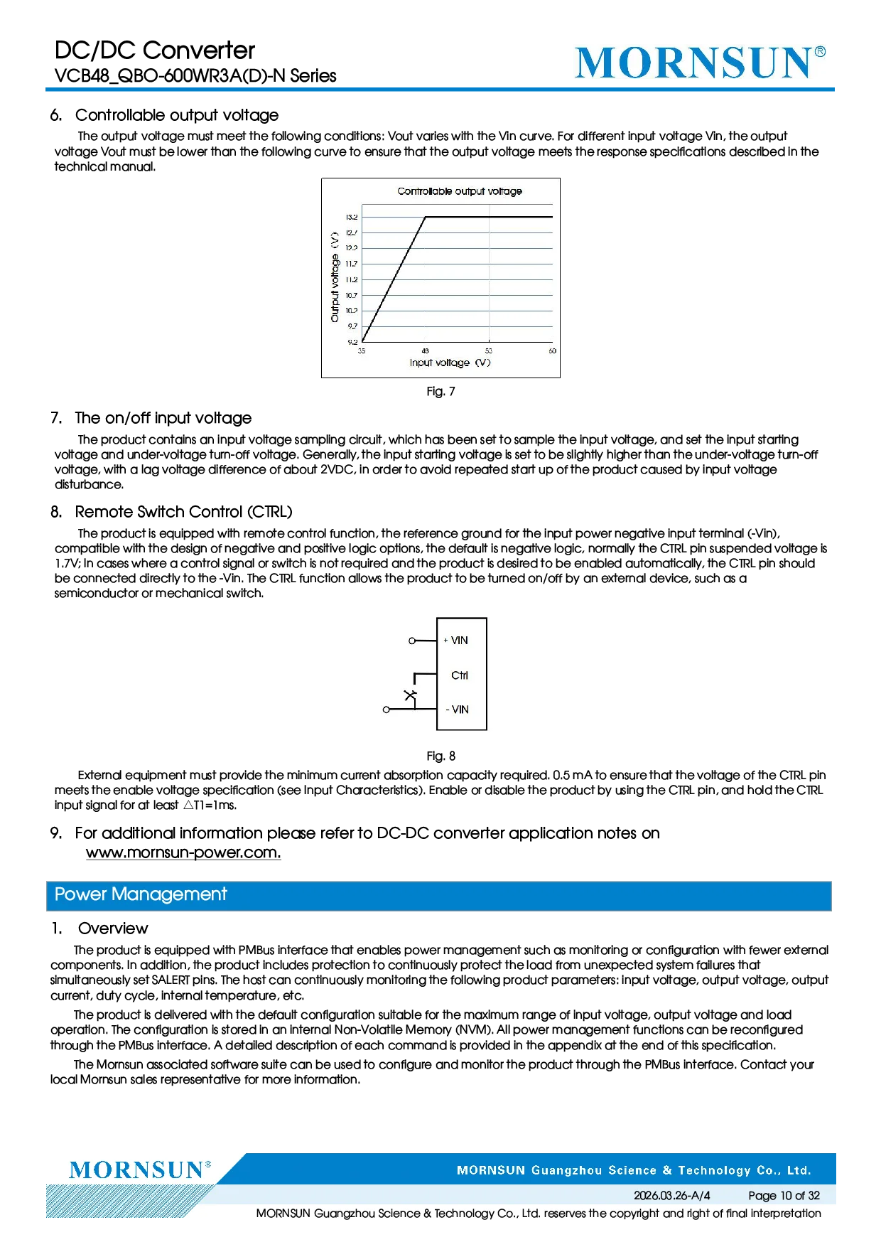
| 6. Controllable output | voltage |
|---|
| The output voltage must | meet the following conditions: Vout varies with the Vin curve. For different input voltage Vin, the output |
|---|
| voltage Vout must be lower | than the following curve to ensure that the output voltage meets the response specifications described in the |
|---|
| technical manual. | Fig. 7 |
|---|
| 7. The on/off input | voltage |
|---|
| The product contains an | input voltage sampling circuit, which has been set to sample the input voltage, and set the input starting |
|---|
| voltage and under-voltage | turn-off voltage. Generally, the input starting voltage is set to be slightly higher than the under-voltage turn-off |
|---|
| voltage, with a lag voltage | difference of about 2VDC, in order to avoid repeated start up of the product caused by input voltage |
|---|
| 8. Remote Switch Control | (CTRL) |
|---|
| The product is equipped | with remote control function, the reference ground for the input power negative input terminal (-Vin), |
|---|
| compatible with the design of | negative and positive logic options, the default is negative logic, normally the CTRL pin suspended voltage is |
|---|
| 1.7V; In cases where a control | signal or switch is not required and the product is desired to be enabled automatically, the CTRL pin should |
|---|
| be connected directly to the | -Vin. The CTRL function allows the product to be turned on/off by an external device, such as a |
|---|
| semiconductor or mechanical | switch.; Fig. 8 |
|---|
| External equipment must | provide the minimum current absorption capacity required. 0.5 mA to ensure that the voltage of the CTRL pin |
|---|
| meets the enable voltage | specification (see Input Characteristics). Enable or disable the product by using the CTRL pin, and hold the CTRL |
|---|
| 9. For additional information | please refer to DC-DC converter application notes on |
|---|
| components. In addition, the | product includes protection to continuously protect the load from unexpected system failures that |
|---|
| simultaneously set SALERT pins. | The host can continuously monitoring the following product parameters: input voltage, output voltage, output |
|---|
| current, duty cycle, internal | temperature, etc. |
|---|
| The product is delivered with | the default configuration suitable for the maximum range of input voltage, output voltage and load |
|---|
| operation. The configuration is | stored in an internal Non-Volatile Memory (NVM). All power management functions can be reconfigured |
|---|
| through the PMBus interface. A | detailed description of each command is provided in the appendix at the end of this specification. |
|---|
| The Mornsun associated | software suite can be used to configure and monitor the product through the PMBus interface. Contact your |
|---|
| local Mornsun sales representative | for more information. |
|---|
| The product provides a | PMBus digital interface that users can configure devices operation as well as monitor input and output voltages, |
|---|
| output currents, and device | temperature. The product can be compatible with any standard two-wire I2C(master must allow for clock |
|---|
| stretching) or PMBus host device. | For the communication protocol operation guide, refer to SMBus Specification Version 3.0. In addition, the |
|---|
| product is compatible with PMBus | version 1.3 and includes an SALERT line to help mitigate bandwidth constraints associated with continuous |
|---|
| failure monitoring. The product | only supports 100 kHz and 400 kHz bus clock frequency. The PMBus signals, SCL, SDA, and SALERT require |
|---|
| passive pull-up resistors as specified | in the SMBus specification. To ensure the rise time, a pull-up resistor is needed: |
|---|
| Where, Rp is the pull-up | resistance and Cp is the parasitic capacitance of the bus. For details, see PMBus 5 11 3 1 0 19 446.16 178.35 34.19 10.22 100 Electrical 5 11 3 1 0 20 482.52 178.35 56.64 10.22 100 Specifications. The |
|---|
| maximum allowed bus capacitance | is 400pF. The pull-up resistor should be connected to an external power supply between 2.7-3.8V. |
|---|
| When communicating via | PMBus, it is recommended to always use PEC(Packet Error Checking) to increase the robustness of |
|---|
| The following address resistor | connection diagram and table show the recommended resistor values for the minimum and maximum |
|---|
| voltage range of hard-wiring | PMBus addresses. (±1% tolerance resistor is recommended); SA0/SA1 Index R (KΩ) R (KΩ); 0 1; 0 24.9 24.9; 1 49.9 49.9; 2 75 75; 3 100 100; 4 124 124; 5 150 150; 6 174 174; Fig. 9; 7 200 200 |
|---|
| The PMBus address can be | configured by SA0 and SA1 pins. The formula is as follows: |
|---|
| PMBus address (decimal) | =8 x SA1 index + SA0 index |
|---|
| If the calculated PMBus | address is 12, 127, or 255, the PMBus address is assigned instead as 0. From a system perspective, users should |
|---|
| also be aware of further restrictions | on addresses as described in the PMBus specification. It is not recommended to keep the SA0 and SA1 |
|---|
| See Fig. 10 below for setting | and holding time timing.; Fig. 10 |
|---|
| The setup time, t , is the | time data, SDA, must be stable before the rising edge of the clock signal, SCL. The hold time thold, is the time |
|---|
| data, SDA, must be stable after | the rising edge of the clock signal, SCL. If these times are violated incorrect data may be captured or |
|---|
| meta-stability may occur and | the bus communication may fail. All standard SMBus protocols must be followed, including clock stretching. |
|---|
| This product supports the BUSY | flag in the status commands to indicate product being too busy for SMBus response. A bus-free time delay |
|---|
| between every SMBus transmission | (between every stop & start condition) must occur. Refer to the SMBus specification, for SMBus electrical |
|---|
| and timing requirements. Note | that an additional delay of 5 ms has to be inserted in case of storing the RAM content into the internal |
|---|
| 5. Monitoring through | PMBus |
|---|
| It is possible to continuously | monitor a wide variety of parameters through the PMBus interface. These include, but are not limited to, the |
|---|
| parameters listed in the table | below.; Parameter PMBus Command; Input Voltage READ_VIN; Output Voltage READ_VOUT; Output Current READ_IOUT; Temperature READ_TEMPERATURE_1; Switching Frequency READ_FREQUENCY; Duty Cycle READ_DUTY_CYCLE |
|---|
| Fault conditions can be | detected using the SALERT pin, which will be asserted low when any number of pre-configured fault or warning |
|---|
| conditions occurs. The SALERT | pin will be held low until faults and/or warnings are cleared by the CLEAR_FAULTS command, or until the |
|---|
| output voltage has been | re-enabled. It is possible to mask which fault conditions should not assert the SALERT pin by the command |
|---|
| SMBALERT_MASK. In response | to the SALERT signal, the user may read a number of status commands to find out what fault or warning |
|---|
| condition occurred, see table | below.; Fault or Warning Status PMBus Command; General Condition Of; STATUS_BYTE、 STATUS_WORD; Equipment; Output Voltage STATUS_VOUT; Output Current STATUS_IOUT; Input Voltage STATUS_INPUT; Temperature STATUS_TEMPERATURE; PMBus Communication STATUS_CML |
|---|
| 7. Non-volatile memory | (NVM) |
|---|
| The product contains a | non-volatile memory region for storing PMBus command values. NVM preloads the Mornsun defaults, which are |
|---|
| writable and customizable, and | can be restored with the command RESTORE_DEFAULT_ALL (0x12). Values in NVM are loaded during |
|---|
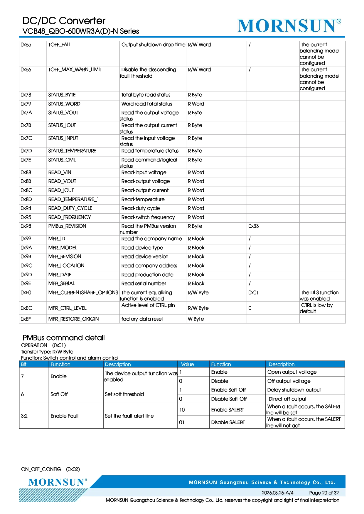
| 8. PMBus switch control | (PMBus CTRL) |
|---|
| PMBus CTRL can be configured | as a switch control through the PMBus interface. PMBus CTRL is disabled and suspended by default. The |
|---|
| logical options controlled by | PMBus CTRL can be positive or negative, and are configured using the OPERATION(0x02) command. When this |
|---|
| feature is not used, it is | recommended that the CTRL pin be connected to DGND. |
|---|
| 9. PMBus configuration | and support |
|---|
| The Mornsun associated software | suite can be used to configure and monitor the product through the PMBus interface. Contact your local |
|---|
| Mornsun sales representative | for more information. |
|---|
| 10. PMBus adjust the | output voltage |
|---|
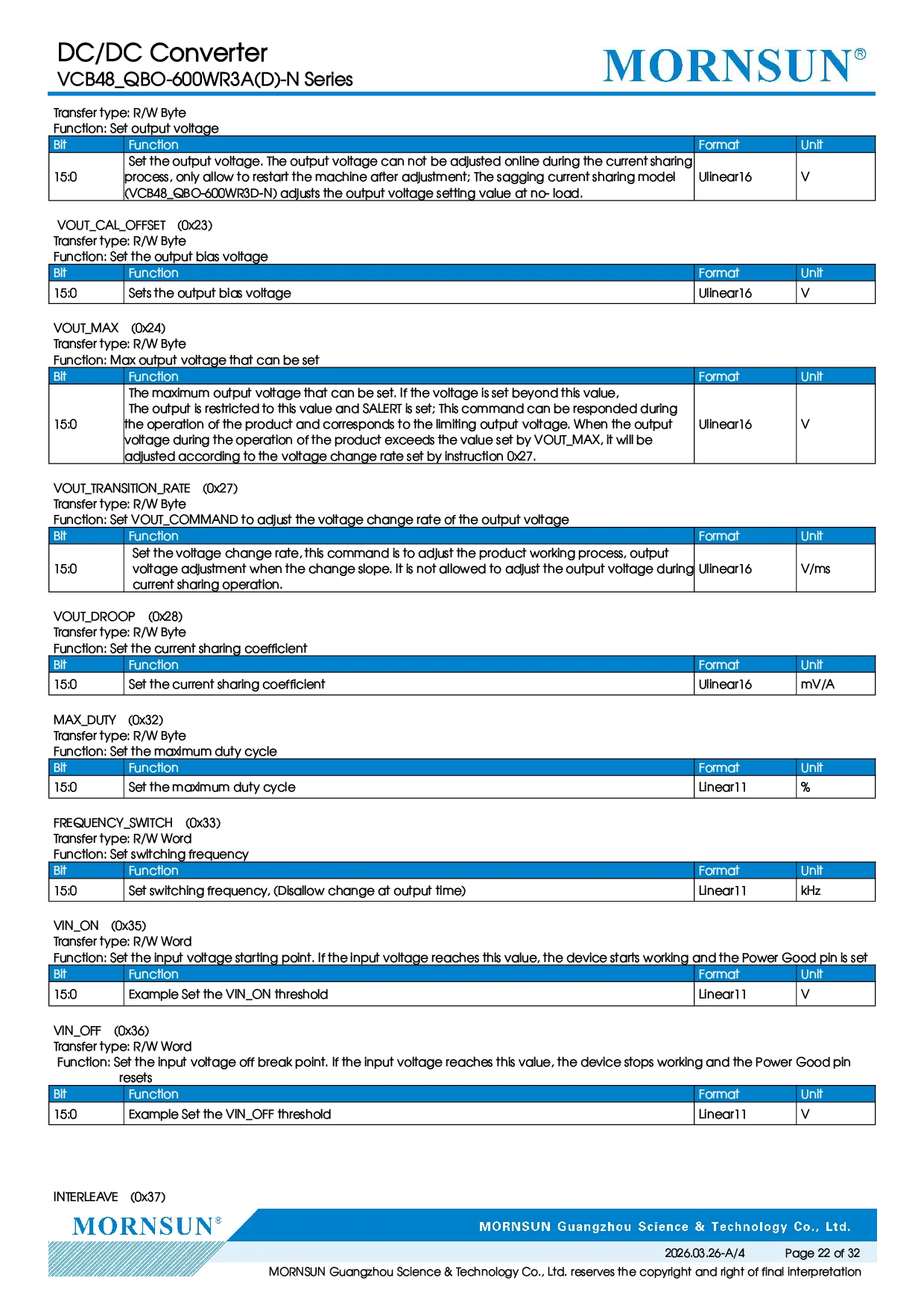
| The output voltage of the | product can be reconfigured using the PMBus command VOUT_COMMAND (0x21) or VOUT_OFFSET (x23). This can |
|---|
| be used to adjust the output | voltage above or below the initial setting of the output voltage to a certain level. See Design Reference -6 |
|---|
| Controllable Output Voltage | Curve for an understanding of the adjustable range of output characteristics. When increasing the output |
|---|
| voltage, the input voltage must | remain within the region plotted, as shown in the figure below. The output voltage setting must be kept |
|---|
| below the over-voltage protection | threshold (OVP) to prevent product downtime. |
|---|
| The following figure marks the | adjustable range of output voltage of the product under the condition of input voltage. Within this range, it is |
|---|
| not fully guaranteed that the | output voltage characteristics of the product will respond according to the response index of the Output 4 12 38 2 2 0 36.840000 701.190450 431.404700 10.215450 -1 ###LINE### 5 12 38 2 2 0 36.84 701.19 58.21 10.22 100 Characteristics |
|---|
| technical | manual, please refer to Figure 7. Secondly, the output voltage shall not be lower than 8V.; Fig. 11 |
|---|
| 11. Use CTRL/PMBus_CTRL | to enable output |
|---|
| The default rise time for a | single product is 10 milliseconds. When the input supply voltage remains constant, use the CTRL/PMBus_CTRL |
|---|
| pin function to enable the | output. The rise and fall of the output voltage and the time of the output control can be configured through the |
|---|
| soft start and soft off functions | (cannot be configured when the current is uniform). This can be used to control the starting impulse current |
|---|
| and manage the power sequence | of multiple controllers. The rise time TON_RISE (0x61) is the time it takes the output to reach its target |
|---|
| voltage, while the fall time | TOFF_FALL (0x65) is the time it takes the output to fall from its target voltage to 1V (the fall time below 1V is |
|---|
| determined by the output load | and the output capacitive load). TON_DELAY (0x60) sets the delay from output enable until output voltage |
|---|
| begins to rise, and TOFF_DELAY | (0x64) sets the delay from output disable until output voltage begins to fall. |
|---|
| In general, the TOFF_DELAY | (0x64) command is only used to control when the output of the product is turned off by CTRL or PMBus_CTRL, |
|---|
| and the supply voltage Vin of | the product remains constant. The output voltage is turned Off by the input voltage under-voltage or |
|---|
| over-voltage, which cannot | control the Off Delay time and Off Ramp time of the down time. |
|---|
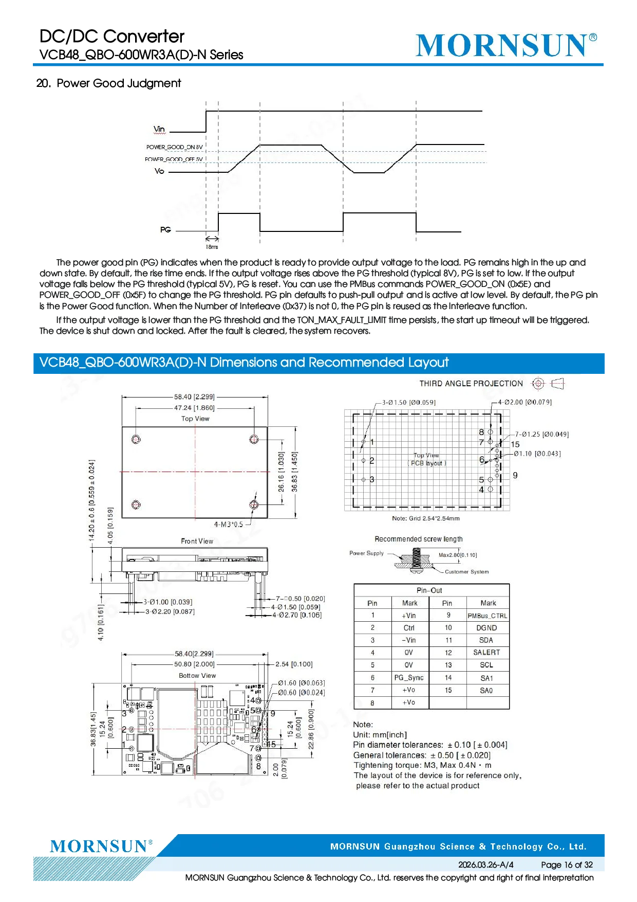
| When the power module | is started by applying the input voltage, there is a minimum 18ms delay from the input voltage to the output |
|---|
| voltage (△T3 -- △T4, normally | 40ms), which is not affected by the CTRL/PMBus_CTRL function. By default, the soft stop is off. When the output |
|---|
| is off, the adjustment of the | output voltage stops immediately. The output voltage drop time is determined by the output load and the |
|---|
| output capacitive load.Soft | shutdown performance can be enabled by using the PMBus command ON_OFF_CONFIG (0x02). You can use |
|---|
| the PMBus commands TON_DELAY | (0x60), TON_RISE (0x61), TOFF_DELAY (0x64), and TOFF_FALL (0x65) to set the delay time and rise/fall time.; Fig. 12 |
|---|
| The product has a Pre-bias | start up functionality and will not sink current during start up if a pre-bias source is present at the output |
|---|
| terminals. If the Pre-bias voltage | is lower than the target value set in VOUT_COMMAND (0x21), the product will ramp up to the target value. |
|---|
| If the Pre-bias voltage is higher | than the target value set in VOUT_COMMAND (0x21), the product will ramp down to the target value and in |
|---|
| this case sink current for a time | interval set by the command TOFF_MAX_WARN_LIMIT (0x66). |
|---|
| Do not allow the output | terminal of the product to be directly connected to the output terminal of other voltage regulator devices in |
|---|
| parallel. In this case, the pre-bias | start up performance may become invalid and the parallel device may be damaged. |
|---|
| 13. Parallel operation | DLS(droop current sharing) |
|---|
| The default VCB48_QBO-600WR3D-N | is delivered with the DLS function. If the required power is equal to or less than the maximum power |
|---|
| of two or more products in | parallel, power redundancy can be realized in parallel. The product provides an output voltage drop |
|---|
| corresponding to a pre-configured | manual resistor in the output circuit, with a default output voltage drop of 200mV from half-load to |
|---|
| full-load for direct shunt. The | output voltage set point is no-load When the load current increases, the output voltage will decrease. When |
|---|
| the multichannel products are | connected in parallel, the output voltage of the overloaded prototype can be effectively reduced to |
|---|
| balance the load of each | parallel prototype. This feature allows products to be connected in parallel and share current with 10% accuracy |
|---|
| at maximum output power. This | means that each module can use up to 90% of its maximum rated current. When the output current sharing |
|---|
| accuracy needs to be improved, | the droop amplitude can be increased by the VOUT_DROOP (0x28) instruction, as described in the PMBus |
|---|
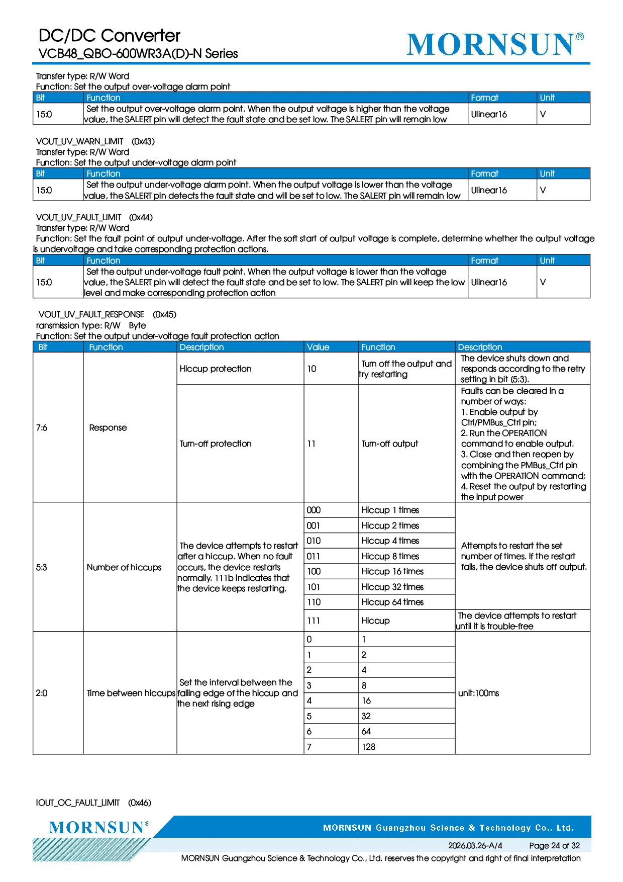
| EMV-Emissionen | CE: CISPR32/EN55032 CLASS A (see Fig. 4-1 for recommended circuit)/CLASS B (see Fig. 4-2 (for recommended circuit)); |
|---|
| EMV-Störfestigkeit | ESD IEC61000-4-2: Contact ±4KV (see Fig.4-2 for recommended circuit) (perf.Criteria B); RS IEC61000-4-3: 10V/m (see Fig.4-2 for recommended circuit) (perf.Criteria A); CS IEC61000-4-6: 10Vr.m.s (see Fig.4-2 for recommended circuit) (perf.Criteria A) |
|---|