| Série | TDA51S485HC |
|---|
| Modelo | TDA51S485HC |
|---|
| Marca | MORNSUN |
|---|
| Differential drive output | Driver; No load, SEL at low or: floating. 3.09–3.62; V: 4.50–5.43; OD; R =54Ω, Figure 7, SEL at low: or floating. 1.17 1.4; L; R =54Ω, Figure 7, SEL at: 2.5 typ, high 1.9 min; L |
|---|
| Differential driver(With load) | |V |: 1.4 typ, 1 min |
|---|
| output | OD3 |
|---|
| OD | ∆V: -0.2–0.2 |
|---|
| states | OD |
|---|
| Common-Mode output voltage | V: 7 1–3; OC |
|---|
| OC | ΔV: 7–0.2 |
|---|
| High input threshold voltage | V: 2; IH |
|---|
| Low input threshold voltage | V: 0.8; IL |
|---|
| Input leakage current | I: -20–20 uA; IL |
|---|
| High-impedance output leakage | DE=0, RE=0,V =0 or 5V,V: =12V–100; CC: IN; I |
|---|
| current | OZ; DE=0, RE=0,V =0 or 5V,V: -60 typ, =-7V -100 min; CC: IN |
|---|
| Output short-circuit | DE= RE=1, TXD=1,; I: 29–62 mA |
|---|
| current(V =HIGH) | OS1 |
|---|
| O | A B |
|---|
| current(V =LOW) | OS2 |
|---|
| Common mode transient | CMTI: 150 kV/μS typ, 100 kV/μS min |
|---|
| immunity | CM; V = V / 2 + 0.4×sin(2πft), |
|---|
| Input capacitance | C: 2 pF; I; CC; Receiver |
|---|
| Positive differential input | V IT(+): -100 typ, -20 max mV |
|---|
| threshold voltage | CM |
|---|
| Negative differential input | V IT(–): -130 typ, –200 min mV |
|---|
| IT+ IT– | CM |
|---|
| RXD output high voltage | V OH: V Vcc − 0.4 Vcc − 0.2; OUT A B |
|---|
| RXD output low voltage | V OL: −0.2 V–0.4; OUT A B; V or V =12V, other pins connect: to 0V–0.1; A B; V or V =12V, power off ,: other pins; A B: 0.06 typ, 0.13 max; connect to 0V |
|---|
| Bus input current | I; I; V or V =–7V, other pins connect: -0.04 typ, to 0V -0.1 min; A B; V or V =–7V, power off ,: other pins; A B: -0.03 typ, -0.1 min; connect to 0V |
|---|
| Input high voltage leakage | I: 20 |
|---|
| current (RE) | IH |
|---|
| Input low voltage leakage | I: -20 |
|---|
| Differential input resistance(A, | R ID: 384–478 kΩ; CM; f = 1.5 MHz, Vpp=1V Sin: Signal, |
|---|
| Differential input capacitance | C D: 7 pF; measure C; D |
|---|
| Input to ground capacitance | C: 2 pF typ, 1MHz min; I |
|---|
| and safeguard characteristic | Power supply |
|---|
| Isolated power supply output | V =5V, no load, SEL=0 or: floating 3.17–3.53 V; CC; V |
|---|
| voltage | ISO; V =5V, no load, SEL=1: 4.50–5.43 V; CC; No load, V =3.3V, RE=0, DE=1,: DI=0,; CC: 10–19; SEL=0; No load, V =5.0V, RE=0, DE=1,: DI=0, |
|---|
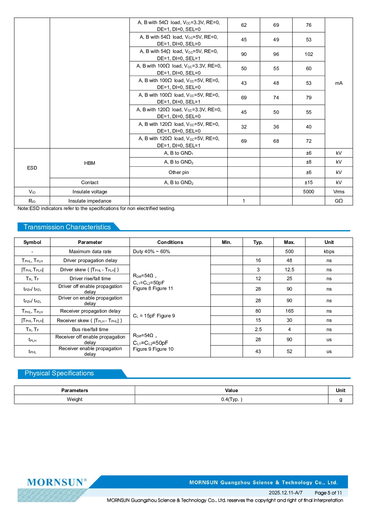
| HBM | A, B to GND: ±8 kV; 2; ESD; Other pin: ±6 kV |
|---|
| Contact | A, B to GND: ±15 kV; 2 |
|---|
| Insulate voltage | V: 5000 Vrms; IO |
|---|
| Insulate impedance | R: 1 GΩ; IO |
|---|