| Série | TD051SCANH3 |
|---|
| Modelo | TD051SCANH3 |
|---|
| Marca | MORNSUN |
|---|
| V , V Supply Voltage | −0.5–6 V |
|---|
| V Input Voltage (TXD) | −0.5–V + 0.5 |
|---|
| I | DD1 |
|---|
| V Output Voltage (RXD) | −0.5–V + 0.5 |
|---|
| O(RXD) | DD1 |
|---|
| V Output Voltage( V | ) −0.5–V + 0.5 |
|---|
| O(SENSE) | DD2SENSE–DD1 |
|---|
| V , V Arbitrary bus terminal voltage | (CANH, CANL) −40 40 V |
|---|
| V Reference Voltage Output | Value −0.5–+6 |
|---|
| T Operating temperature | range −40 to 125°C |
|---|
| T Storage temperature | range −65 to 150°C |
|---|
| stg | Peak temperature Tc ≤ 260°C, time above 217°C max. 60s. For practical |
|---|
| Reflow temperature | application, please refer to IPC/JEDEC J-STD-020D.3 standard. |
|---|
| V Logic Input High | TXD Pinout, Figure11: 2V |
|---|
| V Logic Input Low | TXD Pinout,Figure11: 0.8V |
|---|
| I , I CMOS Logic Input Current | TXD Pinout,Figure 11: 20 uA max |
|---|
| Implicit differential output | bus |
|---|
| V ,V | V = high, R = ∞,Figure: 11 2.0–3.0 V |
|---|
| CANL CANH voltage | TXD L |
|---|
| CANH dominant differential | output |
|---|
| V | V = low, Figure11: 2.75–4.5 V |
|---|
| CANH bus voltage | TXD |
|---|
| CANL dominant differential | output |
|---|
| CANL bus voltage | TXD; V = low, R = 50 Ω, Figure: 11 1.5–3 V; TXD L |
|---|
| OD | V = high, R = ∞, Figure: 11 −50–+50 mV; TXD L |
|---|
| V Positive Input Threshold | 900mV |
|---|
| V Negative Input Threshold | 500mV |
|---|
| IT- | V Hysteresis voltage (VIT+ - VIT-) Figure 14: 150mV |
|---|
| R Bus differential input | impedance: 10–100 kΩ |
|---|
| V Logic output low | I = 1.5 mA: 0.2V typ, 0.4V max |
|---|
| OL | OUT |
|---|
| V Logic output high | I = −1.5 mA: V − 0.2 typ, V − 0.4 min |
|---|
| OH | OUT: DD1 typ, DD1 min |
|---|
| HBM Mode | CANH, CANL pins to GND: ±8 kV |
|---|
| ESD Contact IEC61000-4-2:Perf. | CANH, CANL: ±2 kV |
|---|
| Criteria B | Input-output, electric strength: test for 1 |
|---|
| V Isolated withstand voltage | 5000 VAC |
|---|
| I-O | minute with a leakage current of: 1mA max |
|---|
| R Insulation impedance | 500VDC: 1000 MΩ |
|---|
| CMTI common mode transient | immunity DD1 CM: 180 kV/μs; magnitude = 800 V |
|---|
| Loop | delay |
|---|
| t t | Figure: 15–200 ns |
|---|
| LOOP1 LOOP2 (TXD input to | RXD output) |
|---|
| TXD propagation | delay time |
|---|
| t | 75 ns typ, 100 ns max |
|---|
| PLHD (TXD input to bus | dominant output) |
|---|
| PHLD (TXD input to bus | recessive output) |
|---|
| t , t Differential output | signal rise,fall time: 30 ns typ, 60 ns max |
|---|
| t Bus dominant | time-out time: 0.3 ms typ, 5 ms max |
|---|
| RXD propagation | delay time |
|---|
| PLHR (Bus recessive | to RXD output) |
|---|
| PHLR (Bus dominant | to RXD output) |
|---|
| t , t RXD signal | rise,fall time: 2.5 ns typ, 6 ns max |
|---|
| Parameters | Value Unit |
|---|
| Peso | 0.4(Typ.) g |
|---|
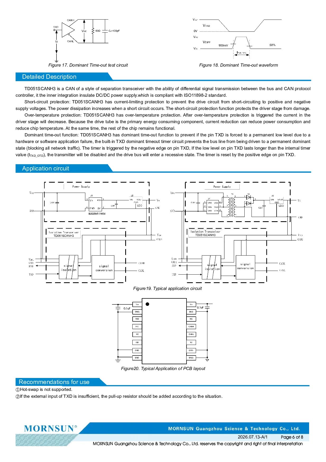
| TD051SCANH3 is a CAN of a style of | separation transceiver with the ability of differential: signal transmission between the bus and CAN protocol |
|---|
| controller, it the inner integration insulate DC/DC | power supply.which is compliant with: ISO11898-2 standard. |
|---|
| Short-circuit protection: TD051SCANH3 | has current-limiting protection to prevent the: drive circuit from short-circuiting to positive and negative |
|---|
| supply voltages. The power dissipation increases | when a short circuit occurs. The short-circuit: protection function protects the driver stage from damage. |
|---|
| Over-temperature protection: TD051SCANH3 | has over-temperature protection. After: over-temperature protection is triggered the current in the |
|---|
| driver stage will decrease. Because the drive | tube is the primary energy consuming: component, current reduction can reduce power consumption and |
|---|
| reduce chip temperature. At the same time, the | rest of the chip remains functional. |
|---|
| Application circuit | Figure19. Typical application: circuit; Figure20. Typical Application of PCB: layout |
|---|
| TD051SCANH3 SOIC | 16: TD051SCANH3–340/RELL |
|---|
| V Supply voltage (control terminal) | 2.375–5.5 V |
|---|
| V Supply voltage (bus terminals) | 4.5–5.5 V |
|---|
| V or V Bus Input Pin Withstand Voltage | (Common Mode) −40 40 V |
|---|
| V TXD high input voltage | 2V |
|---|
| V TXD low input voltage | 0.8V |
|---|
| I Console input quiescent current V | 3.7V typ, 6V max |
|---|
| VDD1_S | = 5.5V, = 5.5V,no |
|---|
| DD1 | DD2 mA |
|---|
| I Bus End input quiescent current | signal–10 |
|---|
| I Console dynamically sends current | V = 5.5V, V =–6 |
|---|
| VDD1_D | DD1 DD2; 5.5V,RL= 60Ω; TXD Pin mA |
|---|
| I Bus End dynamically sends current | Input Signal:f=500kHz;–50 |
|---|
| VDD2_D | Duty=50% |
|---|
| P Total power dissipation V | = 5.5V, V = 5.25V,–300 |
|---|
| D | DD1 DD2 |
|---|
| T A | =105°C, RL= 60Ω; TXD |
|---|
| P Console power dissipation | 30 mW |
|---|