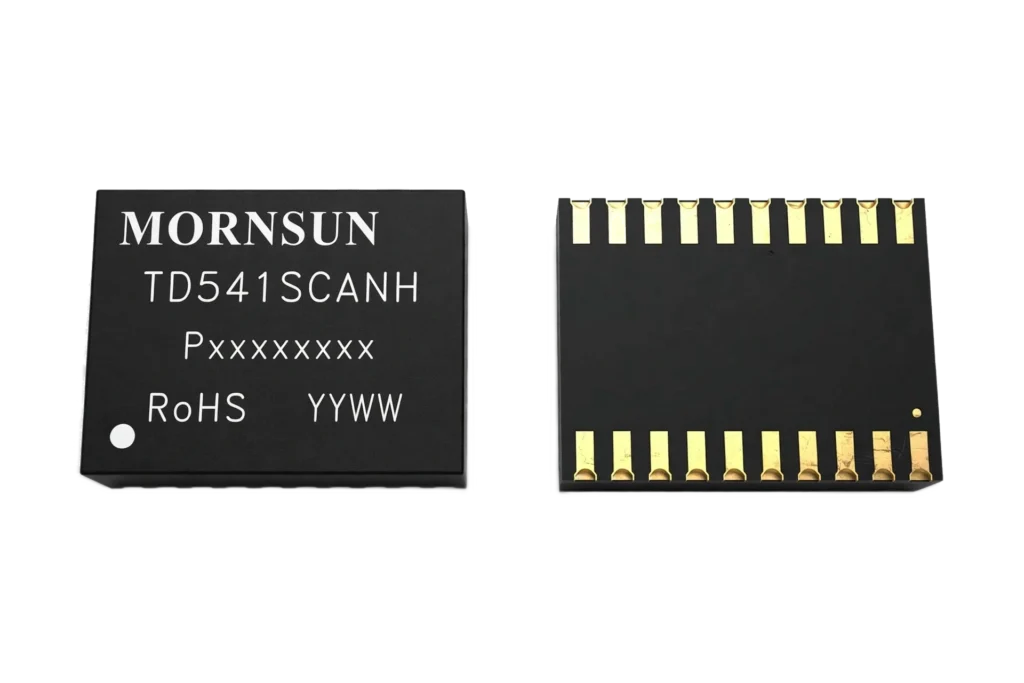
| Dòng sản phẩm | TD541SCANH |
|---|
| Mã hàng | TD541SCANH |
|---|
| Thương hiệu | MORNSUN |
|---|
| Dominant CANH output | voltage: 2.75–3.5 4.5 |
|---|
| |V | | Figure 8 V = 0 V, R =: 60 Ω V |
|---|
| O(D) | TXD L |
|---|
| Dominant CANL output | voltage: 0.5–1.5 2.25 |
|---|
| V Recessive bus voltage | Figure 8 V = 2 V, R = 60: Ω 2–2.5 3 V |
|---|
| O(R) | TXD L; Figure 8 V = 0 V, t < t: , |
|---|
| V | TXD: to(dom)TXD |
|---|
| Differential output voltage | 1.5–3 V |
|---|
| OD(D) | V =4.75 V to 5.25 V, R = 50: to 65Ω; CC L; Figure 8 V = 5 V, R =: 60 Ω –0.12–0.012; TXD L |
|---|
| V Recessive differential output | voltage |
|---|
| OD(R) | V = 5 V, No load: –0.5–0.05; TXD |
|---|
| I TXD High-level input current | V =2 V: 2mA |
|---|
| IH | TXD |
|---|
| I TXD Low-level input current | V =0.8 V: 2mA |
|---|
| IL | TXD |
|---|
| R Internal TXD Pull up Resistor | 9.1 kΩ |
|---|
| V Positive-going input threshold | voltage: 750 900 mV |
|---|
| IT+ | Figure 11 |
|---|
| V Negative-going input threshold | voltage: 500–650 mV |
|---|
| IT– | V Hysteresis voltage ( V - V ): 120mV |
|---|
| hys IT+ | IT –; I = –4 mA, Figure 9: V – 0.4–V – 0.2; OH: IO IO |
|---|
| OH | I = –20 uA, Figure 9: V – 0.4–V – 0.2; OH: IO IO; I = 4 mA, Figure 9: 0.2 0.4; OL |
|---|
| OL | I = 20 uA, Figure 9: 0.2 0.4; OL |
|---|
| C | V = 5 V, V = 0.4 sin (4E6πt): + 2.5 V–13 pF |
|---|
| I (CANH or CANL) | TXD I |
|---|
| C Differential input capacitance | V = 5 V, V = 0.4 sin: (4E6πt)–5 pF |
|---|
| ID | TXD I |
|---|
| R Differential input resistance | V = 5 V: 15–30 40 kΩ |
|---|
| R Input resistance (CANH or | CANL) V = 5 V: 30–80 kΩ |
|---|
| IN | TXD |
|---|
| R | V = V: –3%–0% 3%; I(m) [1 – R / R ] × 100% CANH CANL |
|---|
| IN(CANH) IN(CANL) | CANH, CANL pin to GND: ±15 kV |
|---|
| ESD HBM | Other pins: ±2 kV |
|---|
| EFT IEC61000-4-4:Perf. Criteria | B CANH, CANL and GND: ±2 kV; CANH, CANL and GND(Common |
|---|
| Surge IEC61000-4-5:Perf. Criteria | B: ±2 kV; Mode) |
|---|
| Isolation voltage | 5000 VDC |
|---|
| Insulation Insulation resistance | 1000 MΩ |
|---|
| Isolation capacitor | 3 pF; V = V or 0 V, V = 1 kV,: transient |
|---|
| CMTI Common Mode Transient | Immunity TXD CC CM: 25 kV/us; magnitude = 800 V |
|---|
| Transmission Characteristics | General test conditions and V = V = 5V,: Ta = 25℃ (unless otherwise specified).; CC IO |
|---|
| Parameters | Conditions: Min.–Nom. Max. Unit |
|---|
| t Propagation delay TXD On to bus | active: 80 150 ns |
|---|
| t Propagation delay TXD Off to bus | inactive: 80 200 ns |
|---|
| offTxD | R = 60 Ω, C = 100 pF, see: Figure; L L |
|---|
| t Propagation delay RXD On to | receiver active 10 and Figure 12: 60 300 ns |
|---|
| Propagation delay RXD Off to | receiver |
|---|
| t | 60 250 ns |
|---|
| t Dominant time-out time | C =100 pF: 1.2–3.8 ms |
|---|
| TXD_DTO | L |
|---|
| Trọng lượng | 0.9(Typ.) g |
|---|
| voltage | voltage |
|---|
| TD541SCANH is a CAN of a style of | separation transceiver with the ability of differential: signal transmission between the bus and CAN protocol |
|---|
| controller, it the inner integration insulate DC/DC | power supply. which is compliant with: ISO11898-2 standard. |
|---|
| Short-circuit protection: TD541SCANH has | current-limiting protection to prevent the: drive circuit from short-circuiting to positive and negative supply |
|---|
| voltages. The power dissipation increases when | a short circuit occurs. The short-circuit: protection function protects the driver stage from damage. |
|---|
| Over-temperature protection: TD541SCANH | has over-temperature protection. When: the junction temperature exceeds 160°C, the current in the |
|---|
| driver stage will decrease. Because the drive | tube is the primary energy consuming: component, current reduction can reduce power consumption and |
|---|
| reduce chip temperature. At the same time, the | rest of the chip remains functional. |
|---|
| In General, Vcc and VIo can be shorted(Figure | 14) .If the controller doesn't support 5 signal: input, it can power 3.3V for VIo. |
|---|
| When the module works in normal condition | connect the S foot to GND; 2; Figure15. Port protection circuit for harsh: environments |
|---|
| Component | Recommended part, value Component: Recommended part, value |
|---|
| R3 | 1MΩ D1、D2: 1N4007 |
|---|
| C1 | 1nF, 2kV D3: SMBJ30CA |
|---|
| T1 | ACM2520-301-2P R: 120Ω; terminal |
|---|
| GDT | B3D090L R1、R2: 2.7Ω/2W |
|---|
| protection device. Parameter description lists a | set of recommended circuit parameters,: which can be adjusted according to the actual application |
|---|
| situation. Also, when using the shielded cable, | the reliable single-point grounding of the shield: must be achieved. |
|---|
| V Power supply | 4.75–5 5.25 V |
|---|
| V Power supply(Logic Side) | 2.75–5.25 V |
|---|
| V or V Voltage at any bus terminal (differential | mode) –40–40 V |
|---|
| V High-level input voltage(TXD) | 2V |
|---|
| V Low-level input voltage(TXD) | 0.8V |
|---|
| Receiver | V =5V -4; CC; Driver–70 |
|---|
| T Operating temperature range | -40 to 125°C |
|---|
| CC | f=500kHz;Duty=50% |
|---|
| Signaling rate | 40–1000 kbps |
|---|