| Serie | TD551SCANHS |
|---|
| Modelo | TD551SCANHS |
|---|
| Marca | MORNSUN |
|---|
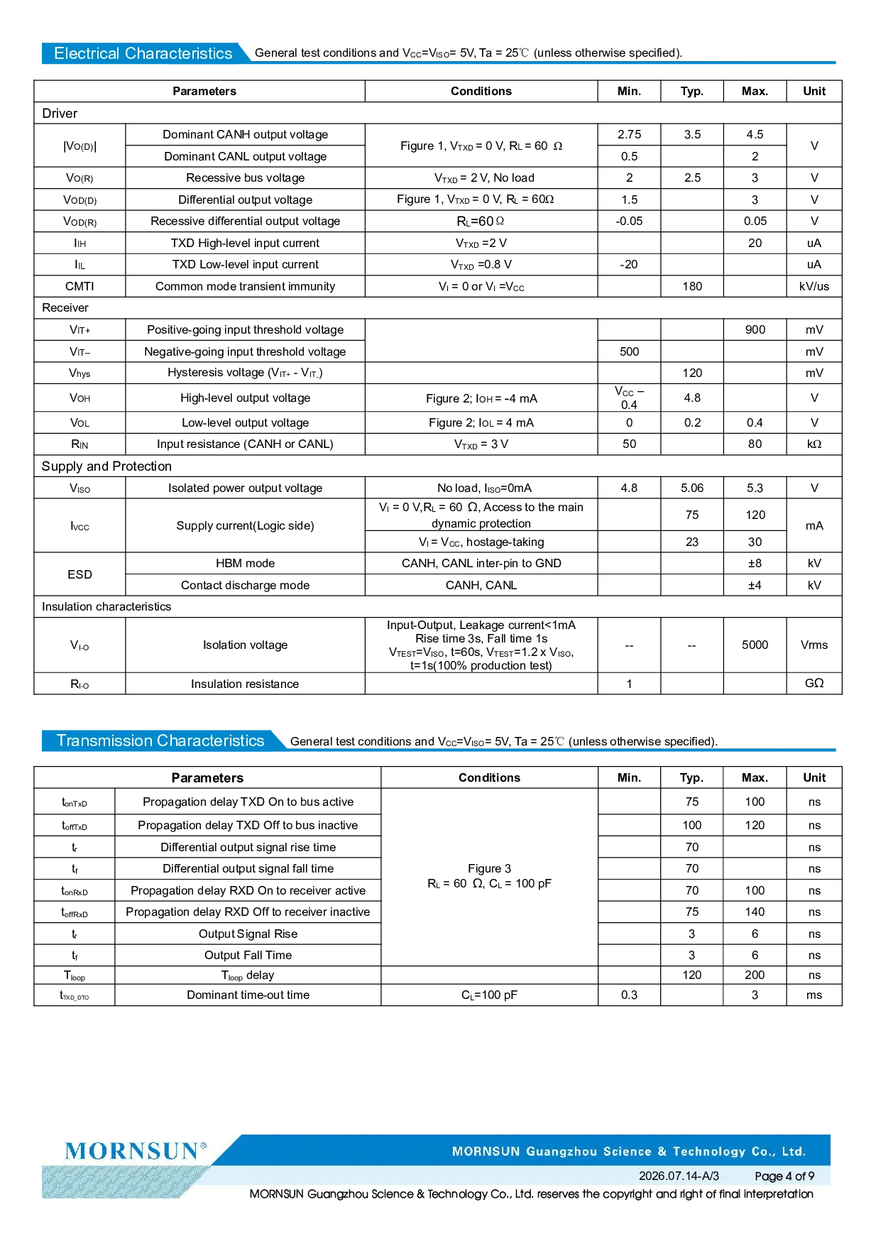
| Dominant CANH output voltage | 2.75–4.5 |
|---|
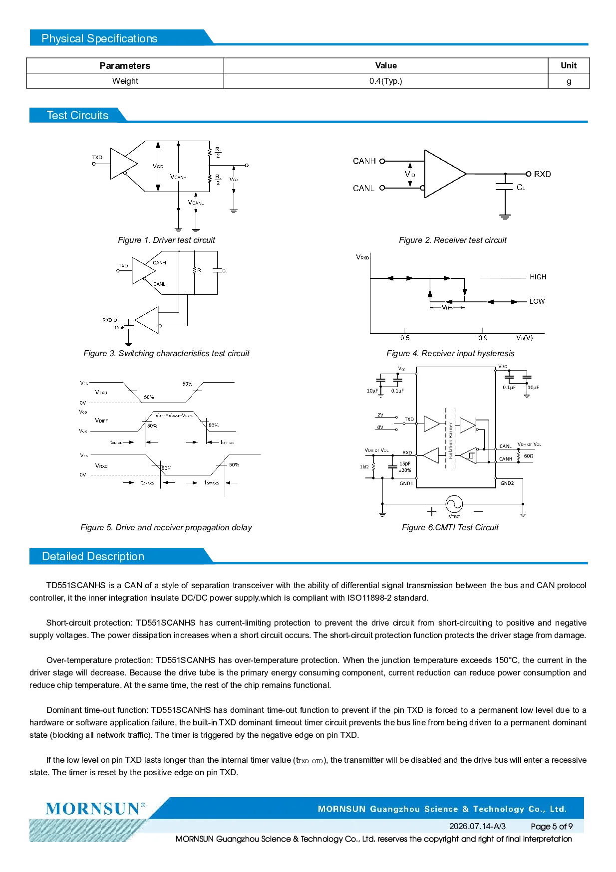
| |V O(D) | | Figure 1, V = 0 V, R L =: 60 Ω V; TXD |
|---|
| Dominant CANL output voltage | 0.5–2 |
|---|
| V O(R) Recessive bus voltage | V = 2 V, No load: 2–3 V; TXD |
|---|
| V OD(D) Differential output voltage | Figure 1, V = 0 V, R =: 60Ω 1.5–3 V; TXD L |
|---|
| V OD(R) Recessive differential output | voltage R =60Ω: -0.05–0.05 V; L |
|---|
| I IH TXD High-level input current | V =2 V: 20 uA; TXD |
|---|
| I IL TXD Low-level input current | V =0.8 V: -20 uA; TXD |
|---|
| CMTI Common mode transient | immunity V = 0 or V =V: 180 kV/us; I I CC |
|---|
| V IT+ Positive-going input threshold | voltage: 900mV |
|---|
| V IT– Negative-going input threshold | voltage: 500mV; V hys Hysteresis voltage (V - V ): 120mV |
|---|
| IT+ | IT –; V – |
|---|
| V High-level output voltage | Figure 2; I = - 4 mA: 4.8V typ, CC min |
|---|
| OH | OH: 0.4 |
|---|
| V OL Low-level output voltage | Figure 2; I OL = 4 mA: 0–0.4 V |
|---|
| R IN Input resistance (CANH or | CANL) V = 3 V: 50–80 kΩ; TXD |
|---|
| V Isolated power output voltage | No load, I =0mA: 4.8–5.3 V |
|---|
| ISO | ISO; V = 0 V,R = 60 Ω, Access to: the main; I L: 75 typ, 120 max |
|---|
| I Supply current(Logic side) | dynamic protection |
|---|
| VCC | V = V , hostage-taking: 23 typ, 30 max; I CC |
|---|
| HBM mode | CANH, CANL inter-pin to: GND–±8 kV |
|---|
| Contact discharge mode | CANH, CANL: ±4 kV |
|---|
| Insulation characteristics | Input-Output, Leakage: current<1mA; Rise time 3s, Fall time: 1s |
|---|
| V Isolation voltage | 5000 Vrms |
|---|
| I-O | V =V , t=60s, V =1.2: x V ,; TEST ISO TEST: ISO; t=1s(100% production: test) |
|---|
| R Insulation resistance | 1 GΩ |
|---|
| Transmission Characteristics General | test conditions and V =V = 5V, Ta =: 25℃ (unless otherwise specified).; CC ISO |
|---|
| Parameters | Conditions: Min.–Max. Unit |
|---|
| t Propagation delay TXD On to bus | active: 75 ns typ, 100 ns max |
|---|
| t Propagation delay TXD Off to bus | inactive: 100 ns typ, 120 ns max |
|---|
| t Differential output signal rise | time: 70 ns |
|---|
| t Differential output signal fall | time Figure 3: 70 ns |
|---|
| f | R = 60 Ω, C = 100 |
|---|
| t Propagation delay RXD On to receiver | active L L: 70 ns typ, 100 ns max |
|---|
| t Propagation delay RXD Off to receiver | inactive: 75 ns typ, 140 ns max |
|---|
| t Output Signal Rise | 3 ns typ, 6 ns max |
|---|
| t Output Fall Time | 3 ns typ, 6 ns max |
|---|
| T T delay | 120 ns typ, 200 ns max |
|---|
| t Dominant time-out time | C =100 pF: 0.3–3 ms |
|---|
| TXD_DTO | L |
|---|
| Peso | 0.4(Typ.) g |
|---|
| TD551SCANHS is a CAN of a style of separation | transceiver with the ability of differential: signal transmission between the bus and CAN protocol |
|---|
| controller, it the inner integration insulate DC/DC | power supply.which is compliant with ISO11898-2: standard. |
|---|
| Short-circuit protection: TD551SCANHS has | current-limiting protection to prevent the: drive circuit from short-circuiting to positive and negative |
|---|
| supply voltages. The power dissipation increases | when a short circuit occurs. The short-circuit: protection function protects the driver stage from damage. |
|---|
| Over-temperature protection: TD551SCANHS | has over-temperature protection. When the: junction temperature exceeds 150°C, the current in the |
|---|
| driver stage will decrease. Because the drive tube | is the primary energy consuming component,: current reduction can reduce power consumption and |
|---|
| reduce chip temperature. At the same time, the rest | of the chip remains functional. |
|---|
| state (blocking all network traffic). The timer is triggered | by the negative edge on pin TXD. |
|---|
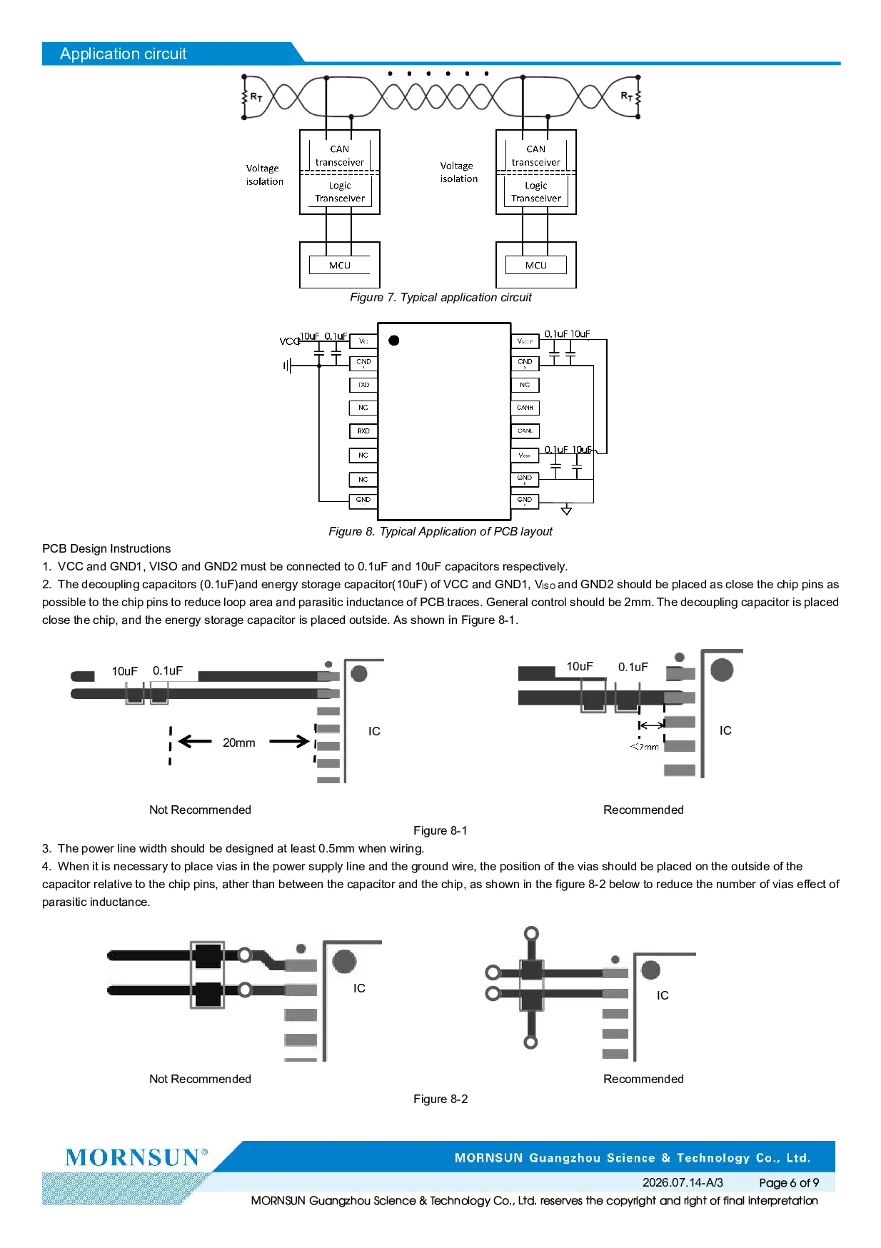
| state. The timer is reset by the positive edge on pin | TXD.; Figure 7. Typical application circuit; Figure 8. Typical Application of PCB layout |
|---|
| 1. VCC and GND1, VISO and GND2 must be | connected to 0.1uF and 10uF capacitors respectively. |
|---|
| 2. The decoupling capacitors (0.1uF)and energy | storage capacitor(10uF) of VCC and GND1,: V and GND2 should be placed as close the chip pins as; ISO |
|---|
| possible to the chip pins to reduce loop area and | parasitic inductance of PCB traces. General: control should be 2mm. The decoupling capacitor is placed |
|---|
| close the chip, and the energy storage capacitor is | placed outside. As shown in Figure 8-1. |
|---|
| 0.1uF | 10uF 0.1uF |
|---|
| 10uF | IC: IC |
|---|
| Not Recommended | Recommended; Figure 8-1 |
|---|
| 3. The power line width should be designed at least | 0.5mm when wiring. |
|---|
| parasitic inductance. | IC; IC |
|---|
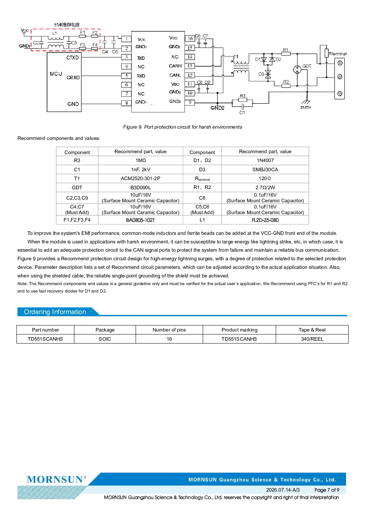
| Component Recommend | part, value Component: Recommend part, value |
|---|
| R3 | 1MΩ D1、D2: 1N4007 |
|---|
| C1 | 1nF, 2kV D3: SMBJ30CA |
|---|
| T1 | ACM2520-301-2P R: 120Ω; terminal |
|---|
| GDT | B3D090L R1、R2: 2.7Ω/2W; 10uF/16V: 0.1uF/16V |
|---|
| C2,C3,C9 (Surface Mount | C8; Ceramic Capacitor): (Surface Mount Ceramic Capacitor) |
|---|
| C4,C7 (Must Add) (Surface Mount | 10uF/16V C5,C6: 0.1uF/16V; Ceramic Capacitor) (Must Add): (Surface Mount Ceramic Capacitor) |
|---|
| F1,F2,F3,F4 | BA0805-102T L1: FL2D-Z5-080 |
|---|
| essential to add an adequate protection circuit to the | CAN signal ports to protect the system: from failure and maintain a reliable bus communication. |
|---|
| device. Parameter description lists a set of Recommend | circuit parameters, which can be adjusted: according to the actual application situation. Also, |
|---|
| when using the shielded cable, the reliable single-point | grounding of the shield must be achieved. |
|---|
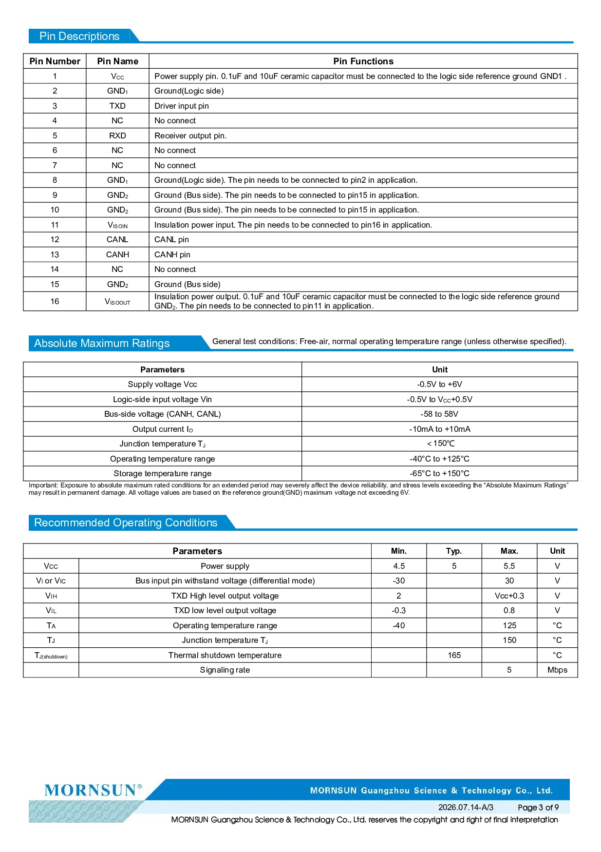
| V CC Power supply | 4.5–5.5 V |
|---|
| V I or V IC Bus input pin withstand voltage (differential | mode) -30–30 V |
|---|
| V IH TXD High level output voltage | 2–Vcc+0.3 |
|---|
| V IL TXD low level output voltage | -0.3–0.8 V |
|---|
| T A Operating temperature range | -40 to 125°C |
|---|
| T J Junction temperature T | 150°C |
|---|
| T Thermal shutdown temperature | 165°C |
|---|
| Signaling rate | 5 Mbps |
|---|