| Series | TD051S422H3 |
|---|
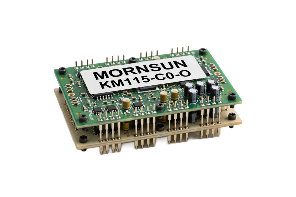
| Model | TD051S422H3 |
|---|
| Brand | MORNSUN |
|---|
| DD2 | — — |
|---|
| Driver Characteristics | R = ∞, Refer to Figure: 7 2 V; L |
|---|
| OD | R = 27 Ω (RS-485), Refer to: Figure 7 1.5 V; L |
|---|
| Amplitude of change of | differential |
|---|
| Δ|V | | R = 27 Ω , Refer to Figure: 9–±0.2 V |
|---|
| OD output | L |
|---|
| Steady state common | mode |
|---|
| V | Refer to Figure 8: 1–3 V |
|---|
| I Driver short-circuit current | -7V ≤ V ≤ 12V: ±110mA typ, ±200mA max |
|---|
| OS | OUT |
|---|
| V Input High Level | — —: 2V |
|---|
| IH | TXD, DE, R E |
|---|
| V Input Low Level | — —: 0.8V |
|---|
| IL | TXD, DE, R E |
|---|
| Negative differential input | threshold |
|---|
| IT(–) voltage | V hysteresis voltage (V IT+ – V IT– ) −7 V ≤ VCM ≤ +12 V: 20mV |
|---|
| R Differential Input Impedance(A,B) | −7 V ≤ VCM ≤ +12 V: 96 kΩ |
|---|
| ID | V: = 12V–280 uA; — — OUT |
|---|
| I Input current (A,B pin) | DE = 0, R E= 0 |
|---|
| I | V: = -7V -100 uA; OUT; I = 20 μA, V − V = 0.2: V V − 0.1; OUT A B: DD1 |
|---|
| OH | I = 4 mA, V − V = 0.2: V − 0.2 typ, V V − 0.4 min; OUT A B: DD1 typ, DD1 min; I = −20 μA, V − V =: 0.2 V–0.1; OUT A B |
|---|
| OL | I = −4 mA, V − V =: 0.2 V–0.4; OUT A B |
|---|
| Power supply and protection characteristics | 2.375 V ≤ V ≤ 5.5: V,; DD1 |
|---|
| I Logic side supply current | 6mA |
|---|
| DD1 | — —; Output without load, R E =: 0 V; Output without load,DE =: 5 V–10 mA; Output without load, DE =: 0 V–10 mA |
|---|
| HBM mode | A, B, Z, Y pins to GND: ±15 kV |
|---|
| ESD IEC/EN 61000-4-2(Contact) | A, B, Z, Y Pin to GND: ±4 kV |
|---|
| Perf. Criteria B | V =V ,t=60s |
|---|
| V Isolated withstand voltage | TEST I-O: 5000 VAC |
|---|
| I-O | V =1.2 x V ,t=1s(100%production: test); TEST I-O |
|---|
| R Insulation impedance | 500VDC: 1000 MΩ |
|---|
| C Isolation capacitors | 5.5 pF |
|---|
| CMTI common mode transient immunity | DD1: 180 kV/μs; magnitude = 800 V |
|---|
| Parameters | Conditions: Min.–Max. Unit |
|---|
| transmission rate | 20 Mbps |
|---|
| t PLH , t PHL Drive Transfer | Delay: 50 ns typ, 90 ns max |
|---|
| Driver Differential | Output Delay; R = 54 Ω, C = C =: 100 pF, |
|---|
| t Offset | L L1 L2: 25 ns |
|---|
| SKEW (|t PHL –t PLH | Reference Figure: 9; |) |
|---|
| t r , t f Driver output rise delay, | fall delay: 6 ns typ, 25 ns max |
|---|
| t PLH , t PHL Receiver transmission | delay: 80 ns typ, 110 ns max |
|---|
| Receiver output rise | delay, fall C = 15 pF, Reference: Figure10; L |
|---|
| t r , t f | 5 ns typ, 10 ns max |
|---|
| Weight | 0.4(Typ.) g |
|---|
| state.The TD051S422H3 adopts a two-terminal | power supply, and the logic side: supports the conversion of 3.3V and 5V logic levels, and the whole |
|---|
| transceiver due to overloading or short-circuit. | transceiver from irreversible damage: caused by bus overload or short circuit. |
|---|
| Receiver input filter: TD051S422H3 | receiver integrated high performance input: filter, the filter can greatly enhance the receiver's noise suppression |
|---|
| ability to high speed differential signal. | Therefore, the transmission delay of the receiver: is also caused by this reason. |
|---|
| Bus Failure Protection: In general, the | bus receiver will be in an indeterminate state: when -220mV < A-B < -20mV. This phenomenon will occur when |
|---|
| a matching resistor on the port. the TD051S422H3 | receiver threshold voltage is relatively: accurate, and the threshold voltage has at least 10mV margin |
|---|
| The bus load capacity (256 point): standard | RS485 receiver input impedance is: defined as 12 kΩ (unit load). A standard RS485 driver can drive at |
|---|
| least 32 load units. TD051S422H3 bus receiver | designed by 1/8 unit load, the input: impedance is greater than 96 kΩ. As a result, the bus allows access |
|---|
| to more transceivers (up to 256). TD051S422H3 | can also be mixed with the standard: RS485 transceiver with 32 unit loads (cumulative receiver load |
|---|
| cannot exceed 32 units). | — — |
|---|
| can be maintained for at least 600ns, the | transceiver will reliably enter into shutdown: mode. |
|---|
| circuit, the module can limit the output current | of the driver within a certain limit. |
|---|
| Using Suggests | Figure 15. Typical Pull-Up and Pull-Down: Resistor Connections |
|---|
| Keep the node in the receiving state only, not | affect the bus. |
|---|
| TD051S422H3 SOIC | 16: TD051S422H3–340/REEL |
|---|